

Multiscale Materials Analysis: From band structure to TEM analysis
Abstract
Abstract
Aim
To investigate the electronic properties and crystal structures and simulate TEM images of materials by computing their Density of States (DOS) and band structures using first-principles methods such as the Density Functional Theory (DFT).
Introduction
In this universe where we humans came about to dwell, we have long sought to understand the materials that shape our world—from the structures we build to the devices in our hands. At the heart of this pursuit lies multiscale materials analysis—a field that connects the atomic-scale structure of materials to their macroscopic properties.
Materials are chosen for specific applications based on unique properties—mechanical, electrical, thermal, magnetic, and more. Understanding why a material behaves the way it does requires digging deep into its atomic arrangement and electronic behaviour.
In our project, we explore the crystal structures of a select few materials, analyse their energy versus distance (E vs r) and force versus distance (F vs r) curves, delve into electronic band structures and densities of states, and perform Transmission Electron Microscopy (TEM) potential field simulations.
The basis of all these is the all-pervasive theory of Quantum Mechanics and its most crucial equation – The Schrödinger Equation (specifically the time-independent Schrödinger equation). Solving the equations for various real-world systems on a case-by-case basis is quite a tedious task, so through the use of computer simulations, it becomes tractable (as always!). In our project, we used ASE (Atomic Simulation Environment) to generate crystal structures with the desired boundary conditions and plot simple E vs r curves for dimers using pre-existing calculators. Calculators, such as EMT (Effective Medium Theory) and GPAW (Grid-Based Projector Augmented Waves), are models based on different theories which provide a methodology to solve the equations, providing reasonably accurate solutions without the overwhelming computational cost of exact methods. For example, GPAW uses a theory known as DFT (Density Functional Theory) to solve many-electron Schrodinger Wave Equations approximately.
It’s important to note that these simulations involve inherent approximations, yielding results that closely—but not perfectly—match experimental values. Higher accuracy would mean solving more complex equations demanding exponentially higher computational power.
This project aims to present a holistic study of materials—emphasising how structure governs properties across different scales and how simulations can bring these connections to light.
Technologies Used
- Atomic Simulation Environment (ASE)
- GPAW
- VESTA
- abTEM
- Python3
Literature Survey
ASE (Atomic Simulation Environment)
The Atomic Simulation Environment (ASE) is a Python library for setting up, running, and analysing atomic simulations. It serves as an interface that instructs calculators (such as GPAW, Quantum ESPRESSO, etc.) on what to simulate, how to perform the simulation, and how to extract the results.
ASE itself does not solve the Schrödinger equation, but it enables users to:
- Build atomic structures (e.g., crystal lattices, molecules, insert vacancies, etc.)
- Assign calculators (e.g., GPAW, Quantum ESPRESSO, LAMMPS)
- Run simulations: optimise geometries, calculate energies, forces, and atomic trajectories
- Analyze results: generate band structures, density of states (DOS), and more
What makes ASE powerful?
- Written in Python, making it easy to use, read, and integrate with other scientific tools
- Compatible with a wide range of calculators, including Quantum ESPRESSO, GPAW, LAMMPS, EMT, VASP, ORCA, and more
- Highly modular and extensible, allowing users to customise workflows and easily add new functionality
GPAW
GPAW represents wavefunctions and electron densities in real space rather than using plane waves or localised orbitals. It reformulates the many-electron Schrödinger equation into a system of single-electron equations, known as the Kohn–Sham equations.
Instead of solving the Schrödinger equation for all electrons directly:
- GPAW uses the Projector Augmented Wave (PAW) method to separate smooth valence electrons from frozen core electrons.
- The PAW method reconstructs the entire wavefunction by adding detailed information only near the atomic nuclei.
GPAW can use either a real-space finite difference grid or plane waves to perform calculations. In our project, we have used the plane wave approach. It operates through a self-consistent field (SCF) loop:
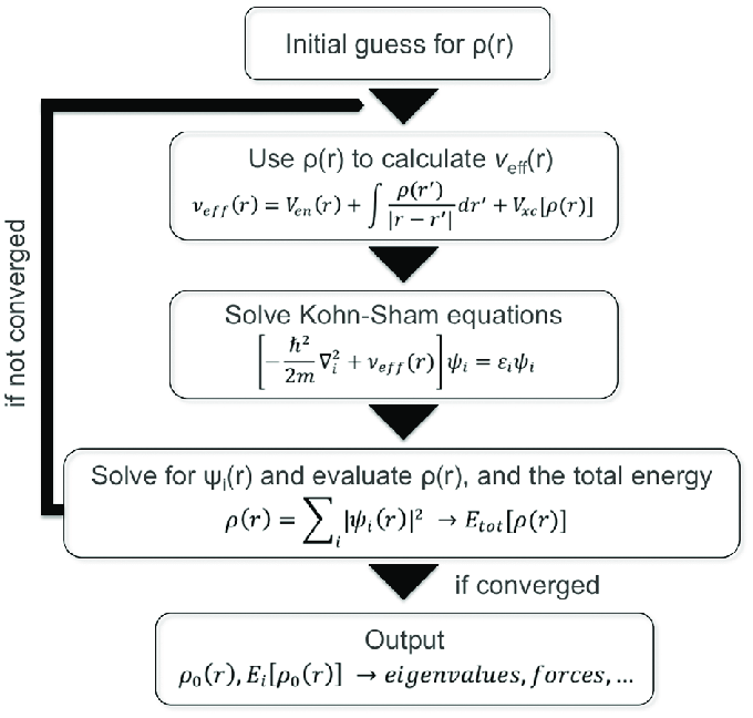
- Guess an initial electron density ρ(r).
- Construct the effective potential V_eff.
- Solve the Kohn–Sham equations → obtain wavefunctions (orbitals) ψᵢ.
- Compute a new density from the orbitals.
- Check for convergence.
Once the wavefunctions and densities converge, GPAW can compute properties such as total energy, atomic forces, band structure, and density of states (DOS).
Why PW method?
In a crystal, atoms are arranged periodically—meaning the potential and electron density repeat across each unit cell. This inherent periodicity is where Bloch’s Theorem becomes essential.
"The wavefunction of an electron in a periodic potential is a plane wave times a periodic function."
According to Bloch’s Theorem, the wavefunction of an electron in a periodic potential can be expressed as:
ψₖ(r) = eᶦᵏʳ · uₖ(r)
where eᶦᵏʳ is a plane wave, and uₖ(r) is a function with the same periodicity as the crystal lattice.
This is precisely why plane waves form a natural and convenient basis for representing electronic wavefunctions in periodic solids—they inherently capture the symmetry and translational invariance of crystalline materials.
What happens while solving using PW?
When using the plane wave basis, the wavefunction is expanded as a sum of plane waves. However, not all plane waves are included—only those with kinetic energy below a specified threshold, called the energy cutoff.
The kinetic energy of a plane wave is given by:
E = ℏ²|G + k|² / 2m
where G is a reciprocal lattice vector and k is the wavevector.
So, for example, choosing PW(500) means that only plane waves with kinetic energy ≤ 500 eV are included.
ℏ²|G + k|² / 2m < E_cutoff
This truncation makes the basis finite and computationally manageable. The process then follows these steps:
- Expand the wavefunction as a sum of the selected plane waves.
- GPAW builds the Hamiltonian Matrix.
- Solve the matrix using linear algebra techniques like iterative diagonalisation.
- Obtain the wavefunctions (eigenstates) and corresponding energy levels (eigenvalues).
VESTA
VESTA (Visualization for Electronic and STructural Analysis) is a go-to tool for visualising crystal structures, surfaces, lattices, and more. It provides an intuitive way to explore the atomic and electronic features of materials.
What one can see in VESTA:
- Atoms are represented with customisable colours and sizes.
- Lattice vectors and coordinate axes.
- Optional visualisation of atomic bonds.
- Creation and visualisation of supercells.
- Symmetry operations within the unit cell.
- Electron isosurfaces (e.g., charge density or orbital shapes).
- Cross-sectional slices along different crystallographic planes.
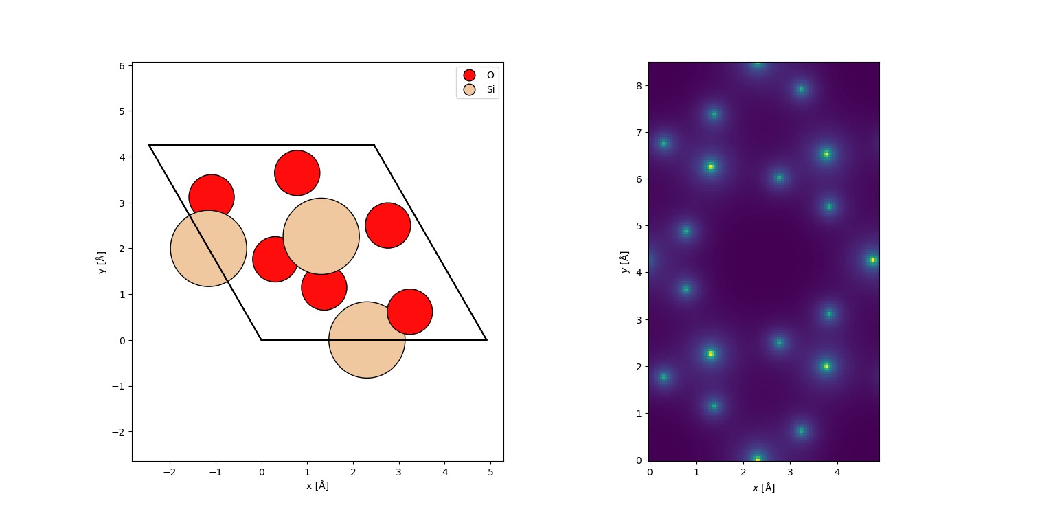
abTEM
abTEM stands for Atomistic Beam-based Transmission Electron Microscopy. It uses atomic coordinates (e.g., from ASE) to simulate how electrons interact with those atoms—generating the images one would get from a real electron microscope.
Why abTEM?
In actual experiments, electron microscopes provide incredibly high-resolution images of materials—down to individual atoms. However, interpreting those images can be challenging. Simulations like abTEM help to:
- Predict how a material will appear under a microscope.
- Understand contrast and features in experimental images.
- Test designs before real-world fabrication.
How does abTEM work?
- Start with an atomic model (typically from ASE).
- Simulate an electron beam passing through the sample.
- Compute the beam's interaction with atoms (elastic/inelastic scattering).
- Reconstruct the image or diffraction pattern observed at the detector.
It uses the Multislice method—a physics-based technique that slices the sample into layers and simulates how the wavefront evolves as it passes through.
The Multislice Method:
- Divide the material into slices.
- Pass an electron wave through each slice.
- Update the wave function at each step.
- Obtain the final image at the end.
Python Programming Language
Python is a high-level, general-purpose programming language. Its design philosophy emphasises code readability with the use of significant indentation. It supports multiple programming paradigms, including structured, object-oriented, and functional programming.
Methodology
ASE Workflow
Building structures :
from ase.build import bulk
si = bulk ('Si', 'diamond', a =5.4)
Assigning calculators:
si.calc = GPAW ( mode ='pw', kpts =(4 , 4 , 4))
si.calc.set ( fixdensity =True ,
                kpts ={ 'path': 'WLGXWK', 'npoints': 100} ,
                symmetry ='off')
Running simulations :
si.get_potential_energy ()
bs = si.calc.band_structure ()
Plotting or analysing results :
bs.plot ( emax =5.0 , filename ='bands_Si .pdf')
Visualising the above workflow:
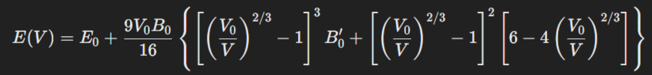
Equation Of States
EOS is a mathematical relationship between fundamental thermodynamic quantities - Pressure, Volume, Temperature - of a material. From the EOS graph, we get:
1. Equilibrium Volume (V0) – Volume at which the system is most stable.
2. Equilibrium Energy (E0) – Total Energy at V0.
3. Bulk Modulus (B0) – Compressibility of material.
The lattice parameter is used to verify the different parameters found.
The theory used: Birch-Murnaghan Equation
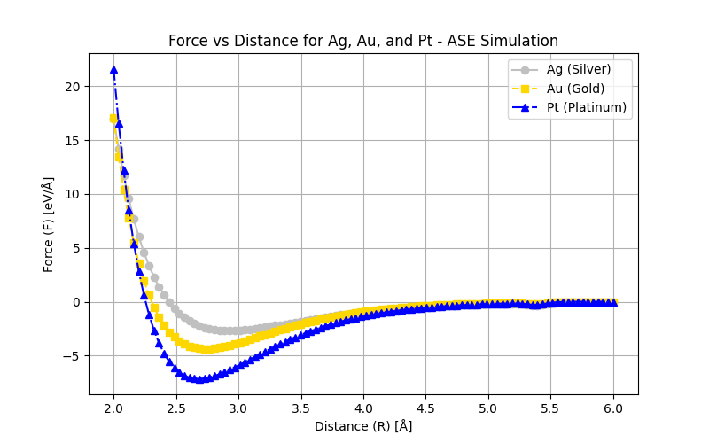
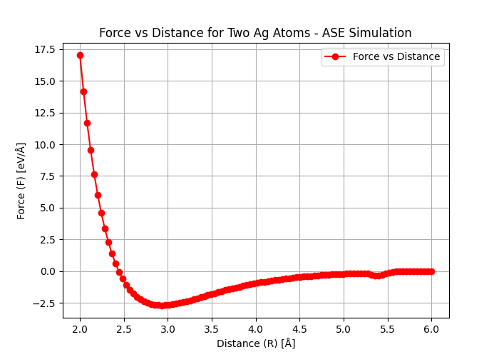
E vs r and F vs r
Several material properties depend on E0, the shape of the interatomic potential curve, and the type of bonding. For example, materials with considerable bonding energies typically have high melting temperatures. At room temperature, substances with considerable bonding energies are usually solids, whereas those with small bonding energies tend to be gases. Liquids generally correspond to bonding energies of intermediate magnitude.
Additionally, the mechanical stiffness (or modulus of elasticity) of a material depends on the shape of its force-versus-interatomic separation curve. The slope of this curve at r = r0 is steep for relatively stiff materials and shallower for more flexible ones.
(FCC metals)
Furthermore, the extent to which a material expands upon heating or contracts upon cooling—represented by its linear coefficient of thermal expansion—is also related to the shape of the E vs r curve. A deep and narrow potential well, typically associated with considerable bonding energies, generally correlates with a low coefficient of thermal expansion and relatively small dimensional changes with temperature.
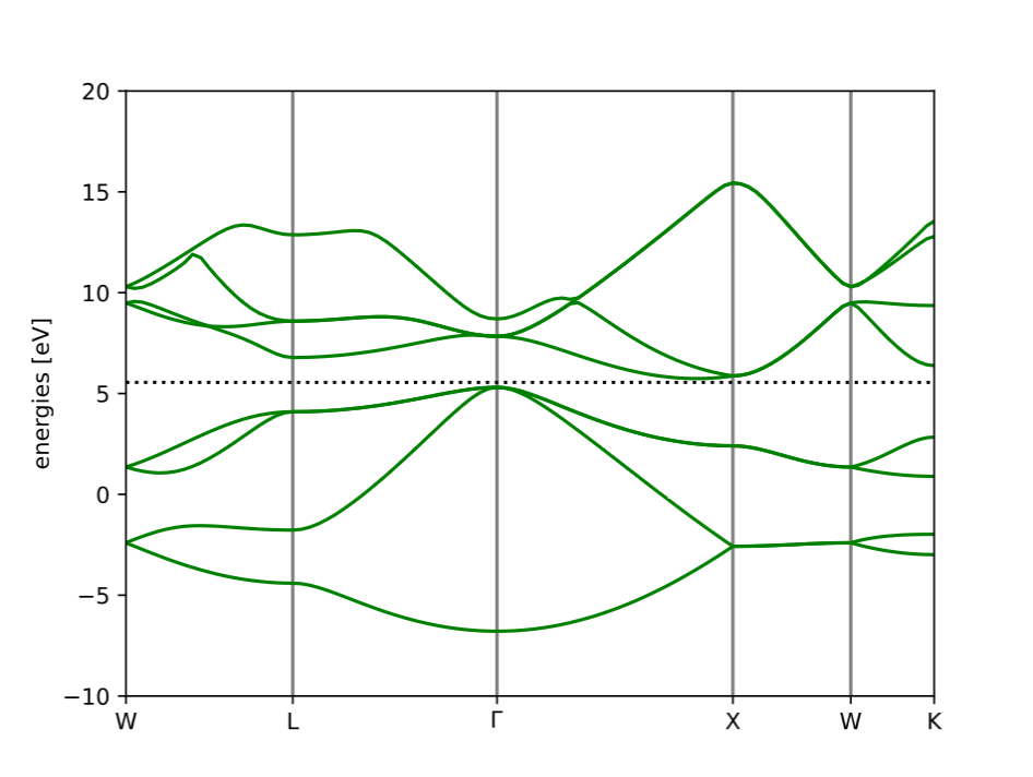
Band Structures
In solid-state physics, a band structure represents the range of energies that electrons in a crystal can occupy and how these energies vary with the electron’s momentum (denoted by k). Unlike isolated atoms, where electrons have discrete energy levels, electrons in a solid experience the periodic potential of the crystal lattice, causing their energy levels to spread into energy bands. Between these bands, there may be band gaps—energy ranges where no electron states exist. This structure is fundamental in determining whether a material behaves as a metal, semiconductor, or insulator.
Band structures are typically visualised as plots of energy (E) versus wavevector (k) along high-symmetry paths in the Brillouin zone (the primitive unit cell in momentum space). In metals, bands cross the Fermi level (the highest occupied energy level at absolute zero), allowing electrons to move freely. In semiconductors and insulators, a band gap separates the valence band (occupied) from the conduction band (unoccupied), and the size of this gap defines the material's electronic behaviour.
Understanding band structures is essential for predicting electrical conductivity and optical properties and for designing materials for electronics, solar cells, or quantum devices.
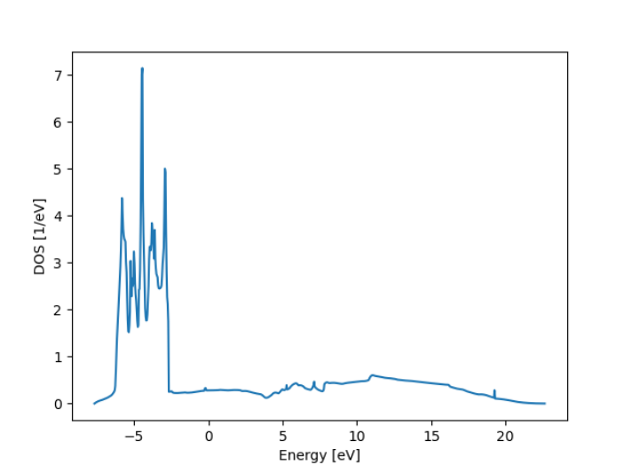
Density of States
The Density of States (DOS) tells us how many electronic states are available at each energy level within a material. It’s essentially a function that describes how densely packed the allowed energy levels are, and it plays a key role in determining a material’s electronic, thermal, and optical properties. While a band structure shows how energy varies with momentum (E vs k), the DOS ignores momentum and focuses purely on how many states exist at each energy, making it especially useful for understanding overall behaviour like conductivity or heat capacity.
In metals, the DOS at the Fermi level (the highest occupied energy at 0 K) is non-zero, meaning electrons can easily be excited and contribute to electrical conductivity. In contrast, semiconductors and insulators have a gap in the DOS at the Fermi level — reflecting the band gap — where no states are available. This gap explains why semiconductors don’t conduct electricity unless energy is provided to move electrons from the valence band to the conduction band.
Results
These are the set of results we obtained for Silver (Ag), a metal with a Face-Centred Cubic (FCC) crystal structure, at room temperature.
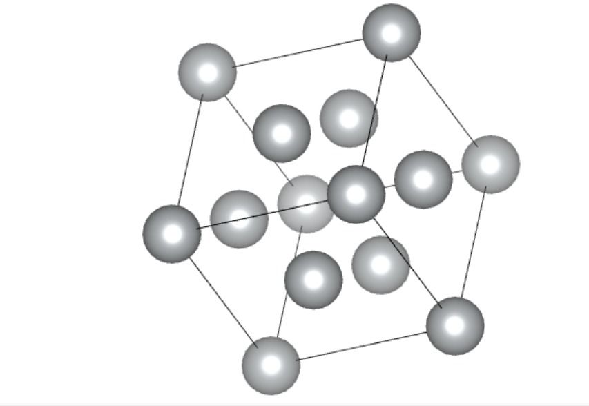
Ag atoms - One Unit Cell - FCC:
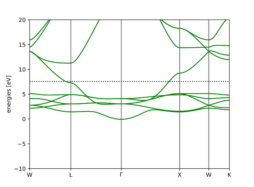
Band Structure of Ag: Being a metal and a good conductor, we can see a significant overlap between the conduction and valence bands, with the absence of a band gap.
EOS Plot.
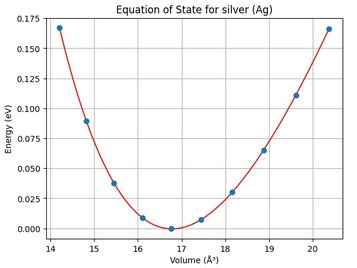
| Element | Equilibrium Energy | Equilibrium Volume | Bulk Modulus | Calculated Lattice Paramater | Actual Lattice Paramater |
| Silver | 0.00 eV | 16.78 Å3 | 0.62 GPa | 4.01 Å | 4.09 Å |
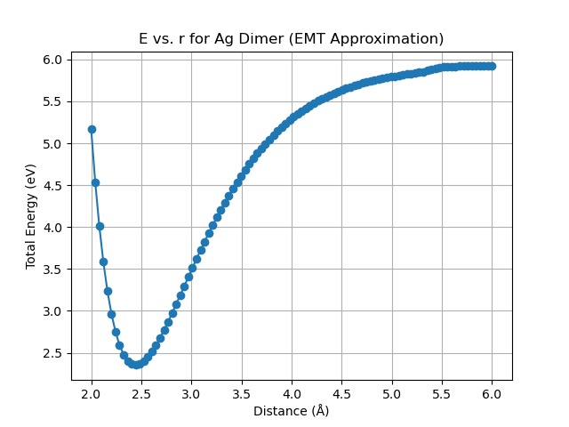
E vs r plot for Ag dimer: we estimated the distance between 2 atoms - turned out to be around 0.24 nm
Density of States - Ag
F vs r for Ag dimer
abTEM Potential Field Maps:

Future Scope
As mentioned earlier, the simulations conducted in this study involve certain approximations. However, they effectively allow us to visualise and interpret key physical phenomena. More advanced computational tools such as Quantum ESPRESSO, LAMMPS, or VASP can be employed for improved accuracy and deeper insights. These platforms can solve more complex equations and account for many-body interactions—though they come with a significantly higher computational cost.
This project primarily focused on metals—especially face-centred cubic (FCC) structures and transition metals—and semiconductors like Si and GaAs. Future studies could broaden this work by exploring more complex and emerging material systems such as:
- Quantum materials, e.g., topological insulators and 2D materials like graphene or MoS₂.
- Battery materials, including Li-ion cathode and anode systems.
- Nanostructured materials, such as quantum dots and nanowires.
- Oxide and perovskite materials - relevant in electronics, catalysis, and photovoltaics.
We have also used VESTA and abTEM to visualise structural features and defects. Future simulation efforts can build upon this by:
- Solving for electronic wavefunctions to obtain band structures and density of states (DOS).
- Exploring defect engineering, e.g., the role of oxygen vacancies in modifying semiconducting behaviour.
- Determining optimal defect concentrations to tune electronic, optical, or catalytic properties.
- Investigating the effects of strain on electronic structure and phase transitions.
- Using molecular dynamics to study thermal stability, diffusion mechanisms, and phonon interactions.
- Integrating machine learning models to predict material properties from simulation data—reducing reliance on costly first-principles calculations.
In summary, the simulation framework established in this project lays a robust foundation for high-fidelity studies across a broad range of advanced materials. With further development, it has the potential to contribute meaningfully to the design and discovery of next-generation materials.
GitHub Repository
All the simulation files and source codes can be found here.
Acknowledgement
As executive members of IEEE NITK, we are incredibly grateful for the opportunity to learn and work on this project under the prestigious name of the IEEE NITK Student Chapter. We want to extend our heartfelt thanks to IEEE for providing us with the funds to complete this project successfully.
Report Information
Team Members
Team Members
Report Details
Created: April 6, 2025, 5:17 p.m.
Approved by: Achinthya Krishna B [Piston]
Approval date: April 7, 2025, 5:02 p.m.
Report Details
Created: April 6, 2025, 5:17 p.m.
Approved by: Achinthya Krishna B [Piston]
Approval date: April 7, 2025, 5:02 p.m.