

2 Level Cache controller on a RISC-V core
Abstract
Abstract
2-Level Cache controller on RISC-V core
Aim
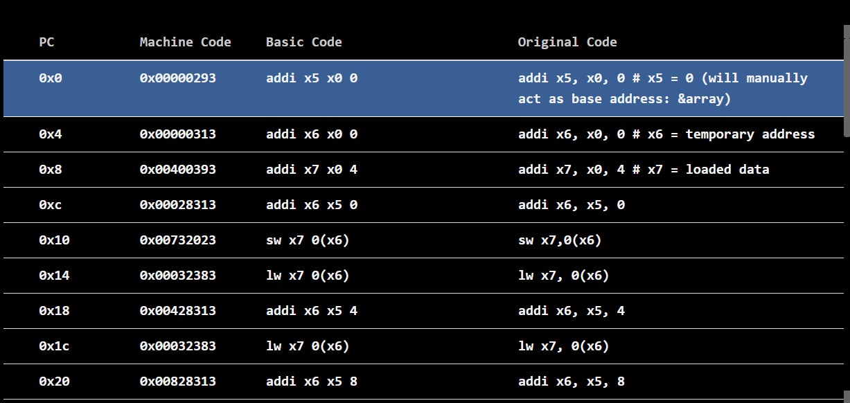
The aim of this project is to develop a pipelined RISC-V processor integrated with a hierarchical cache system to reduce memory access latency. The design includes: A functional RV32I processor core with basic arithmetic, logic, control, and memory instructions. L1 and L2 caches with distinct mapping policies (L1, direct-mapped and L2, 4-way set associative). Implementation of write-back and no-write allocate policies with Least Recently Used (LRU) replacement. Testing and verification of different set of instructions on the integrated work of cache and Single cycle Risc-v that can include a balanced set of Load/Store and Alu instructions.
Introduction
The RISC-V architecture is an open-source instruction set architecture (ISA) that is gaining popularity due to its simplicity and flexibility. This instruction set architecture (ISA) is used for the development of custom processors targeting a variety of end applications. Originally developed at the University of California, Berkeley, the RISC-V ISA is considered the fifth generation of processors built on the concept of the reduced instruction set computer (RISC). Due to its openness and its technical merits, it has become very popular in recent years.
Cache Controller acts as an intermediate between the processor and the cache memory. It executes the read and write requests (Load and Store type instructions) from the RISC-V processor and copies or replaces data within different levels of cache memory and main memory to reduce the average time taken by the processor to retrieve data from an address.We shall be implementing a Cache controlling mechanism with L1 and L2 caches on a Single-cycle RISC-V processor. It will provide hands-on experience with hardware design, digital logic, and microprocessor architecture.
Technologies Used


Xilinx Vivado IDE, Ripes-Riscv Simulator, GTKwave(debugging)
Languages: Verilog HDL, RISCV-asm
Xilinx vivado: AMD Vivado is an FPGA design suite for hardware synthesis, implementation, and verification.
Ripes: An open-source visual simulator for RISC-V that models pipelines, caches, and peripherals. It is used to generate the binary executable file “TEST_INSTRUCTIONS.dat” that will be uploaded to our processor.
GTKwave: A waveform viewer for post-simulation debugging of digital designs. It is more efficient and simpler to use as compared to the traditional testbench method during analysis and debugging for errors.
Literature Survey
Implementation and comparison of different cache mappings
Methodology
Research Phase:
Understanding Memory Hierarchy:
Studied spatial locality (data close in memory) and temporal locality (data frequently accessed) principles to optimize cache design.
Average Memory Access Time (AMAT): Derived formulas to calculate AMAT based on hit/miss rates and penalties: AMAT= Hit time + Miss rate * Miss penalty
Write Policy Analysis: Compared write-through (simpler but slower) vs write-back (complex but faster) approaches.
Design Procedure:
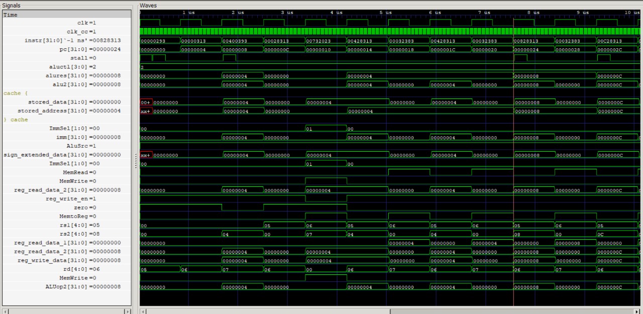
The RV32I processor core was implemented using Verilog HDL with a 5 stage single cycle step which includes:
-Instruction Fetch (IF)
-Instruction Decode (ID)
-Execute (EX)
-Memory Access (MEM)
-Write Back (WB)
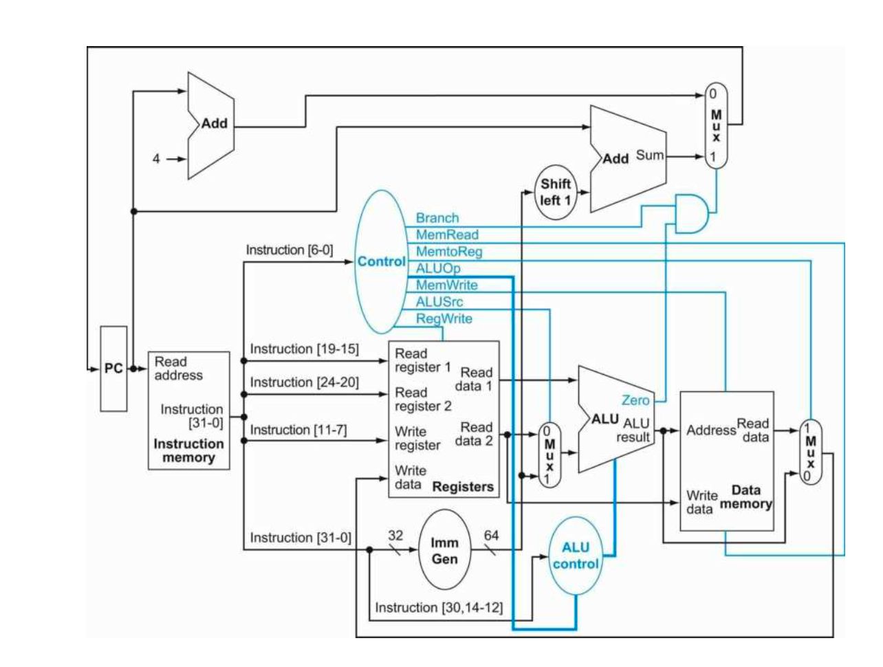
We have followed the Structural modelling methodology wherein, we have defined each element as modules that are instantiated to create the required data path and the control unit block gives the control signals to form the control path.
Cache Design:
The cache has an approximately 5 times higher clock rate as that compared to the RIsc-v processor. This is so because, the memory clock rate should be independent and manifold times faster in order to reduce the AMAT.
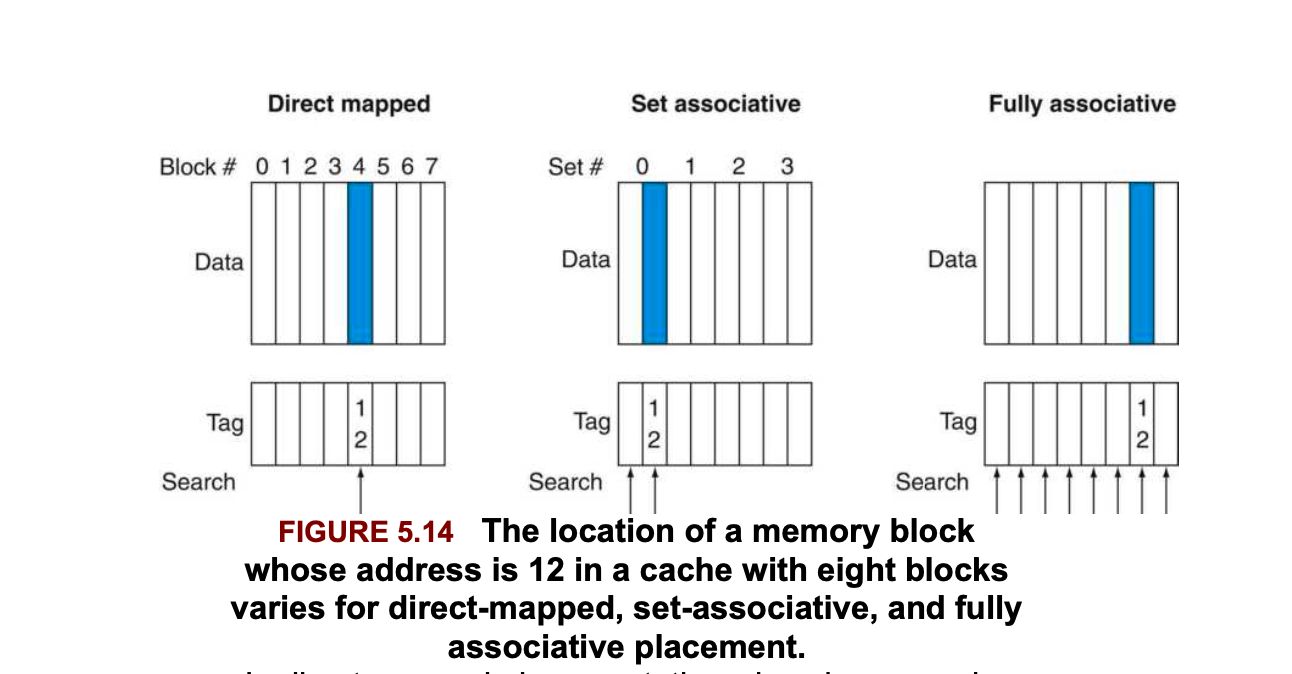
L1-Cache (direct mapped): Total size: 64b. Memory access delay: 1 cycle. This module contains the implementation of the memory for L1 Cache, which briefly contains the memory array, tag array and the valid array. It has been initialized in the module as well.
L2-Cache (4-way set associative): Total size: 512b. Memory access delay: 4 cycles, REPLACEMENT POLICIES: LRU based on accesses made. This module contains the implementation of the memory for L2 Cache, which briefly contains memory array, tag array, LRU array and the valid array. It has been initialized in the module as well.
Main Memory: Total size: 4kb. Memory access delay: 10 cycles
We have implemented the WRITE BACK and NO WRITE ALLOCATE cache policies on these caches.
Implementation:
1. Check Mode (Read/Write): Before processing, check the wait signal to ensure the controller isn’t busy.
2. Read Operation: The controller first checks the L1 Cache.
3. L1 Hit: If found in L1, return data to the processor and set the L1 hit signal.
4. L1 Miss: Search in L2 Cache.
5. L2 Hit: Introduce a 2-cycle delay. If found, promote the block to L1.
6. L1 Promotion: If the L1 location is occupied, evict the existing block. Write it to L2 (if present) or to main memory.
7. L2 Miss: If not found in L2, initiate a main memory search with a 10-cycle delay.
8. Main Memory Fetch: After fetching from main memory, promote to L2 (evict and update if needed), then to L1 (evict and update as before).
9. L1 Promotion (cont.): Evict block from L1 if needed, as in step 6.
10. Deliver Data: Send the fetched data to the processor.
11. Write Operation: First, check if the address is in L1 Cache.
12. L1 Hit on Write: Modify data in L1. Controller is ready for the next instruction.
13. L1 Miss: Check L2 Cache and modify data there if found.
14. L2 Miss: Modify data directly in main memory.
15. Write Policy: No promotion to L1 or L2 on writes (Write No-Allocate). No evictions occurs.
Results
Processor- 11.9Mhz (84ns period)
Cache- 500MHz (2ns period)
Speedup achieved (after L1 full)- 3.75
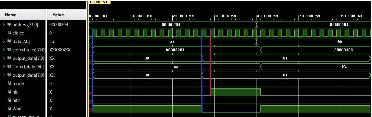
Case 1: Data miss in both L1 and L2 finally read from main memory and then written back to L1 and L2 …
Total Time taken :13 clock cycles.. Marked in Blue
Read from L1 after write back marked in Red. Total Time taken 1 Clock cycle.
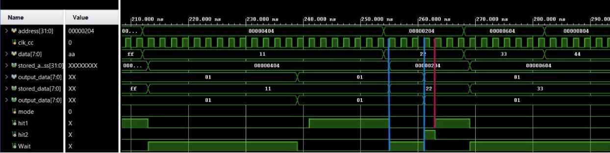
Case 2: Data miss in L1 finally read from L2 and then written back to L1
Total Time taken 3 clock cycles .. Marked in Blue
Read from L1 after write back marked in Red. Total Time taken 1 Clock cycle.
Conclusion and Future Scope
The implemented two-level cache controller effectively reduced average memory access latency by optimizing hit rates at both L1 and L2 levels of the hierarchy. The integration with an RV32I core demonstrated significant improvements in throughput compared to a non-cached baseline design.
1) Firstly, branch prediction can be added to reduce time fetching the wrong instruction.
2) As far as Cache goes, having more sophisticated cache policies like write through and write allocate can also benefit in certain use cases. Even implementing an L3 cache can have certain advantages for modern processors say RISC-V with V extension.
3) Implementing multicore coherence protocols such as MESI or MOESI for shared caches in multicore systems. Exploring adaptive replacement policies like DRRIP or ARC for further improvement in miss rates.
4) Even prefetching mechanisms can be added to reduce compulsory misses during sequential access patterns.
5) Lastly, the entire system can be synthesized on an FPGA of suitable category, so that the power report and other parameters can be realizable on hardware.
References
Hardware Modelling using Verilog
GitHub Repository
All the simulation files and source codes can be found here.
Acknowledgment
As executive members of IEEE NITK, we are incredibly grateful for the opportunity to learn and work on this project under the prestigious name of the IEEE NITK Student Chapter.
Report Information
Team Members
Team Members
Report Details
Created: April 7, 2025, 10:43 a.m.
Approved by: Vishnu M N [Diode]
Approval date: April 7, 2025, 4:54 p.m.
Report Details
Created: April 7, 2025, 10:43 a.m.
Approved by: Vishnu M N [Diode]
Approval date: April 7, 2025, 4:54 p.m.