

16 Point FFT ASIC Flow Design
Abstract
Abstract
1. Introduction
The Fast Fourier Transform (FFT) is a widely used algorithm in digital signal processing (DSP) for converting a signal from its time domain to its frequency domain. It forms the computational backbone of numerous applications such as wireless communication, image processing, radar systems, and audio signal analysis. Implementing an FFT in hardware not only increases speed but also significantly reduces power consumption, making it suitable for real-time embedded systems and ASICs.
This project aims to implement a 16-point FFT using a full ASIC design flow, covering both front-end (RTL design and simulation) and back-end (synthesis to layout) stages. The primary objective is to gain hands-on experience in the complete design and verification cycle of a moderately complex DSP block using industry-relevant tools and open-source technology.
The design is initially developed and simulated using Verilog HDL in Xilinx Vivado to ensure functional correctness. Once validated, the synthesized netlist is taken through the OpenLane flow for physical design using the SkyWater 130nm PDK. Layout visualization and verification are performed using KLayout and Magic VLSI tools. This end-to-end implementation showcases the integration of algorithm-level modeling with ASIC design principles.
The purpose of this project is not only to build a functional FFT core but also to explore real-world VLSI challenges such as timing closure, floorplanning, placement, routing, and layout verification using open-source EDA tools and process design kits (PDKs).
2. Background Theory
2.1 What is FFT?
The Fast Fourier Transform (FFT) is an efficient method to convert a signal from the time domain to the frequency domain. In simple terms, it helps us understand which frequencies are present in a signal, and how strong they are. Instead of doing a large number of calculations like the normal Discrete Fourier Transform (DFT), FFT reduces the number of steps, making it much faster.
For a 16-point FFT, we are analyzing 16 time-domain values and converting them into 16 frequency-domain values.
2.2 Importance of FFT
FFT is used in many real-life applications such as:
Audio processing – to remove noise or improve sound quality
Image processing – for filtering and feature extraction
Wireless communication – like in 4G/5G for OFDM modulation
Medical instruments – such as ECG or MRI analysis
Because of its wide use, having a fast and efficient hardware implementation of FFT is very important.
2.3 Butterfly Operation
The core part of FFT is the "butterfly" structure, which performs a simple combination of addition, subtraction, and multiplication operations between pairs of input points. These butterfly units are repeated in multiple stages depending on the number of points (log₂(N) stages for N-point FFT). For 16-point FFT, we need 4 stages of butterflies.
2.4 What is ASIC Design Flow?
ASIC stands for Application-Specific Integrated Circuit. It means designing a custom chip for a particular task – in this case, for performing a 16-point FFT. The ASIC design flow includes:
Writing the design using HDL (like Verilog)
Simulating to check if it works
Synthesizing it into gates
Creating a physical layout
Checking if the layout follows design rules
Generating the final chip design (GDSII)
2.5 SkyWater 130nm Technology
In this project, we use the SkyWater 130nm PDK – which is an open-source process design kit. It provides the basic information about how the chip will be manufactured, such as:
Standard cell library
Design rules
Layer information for layout
Sky130 is suitable for academic and research projects and helps students learn real chip design using free tools.
3. Design Methodology
This section explains the complete step-by-step process followed during the design and implementation of the 16-point FFT using ASIC design flow.
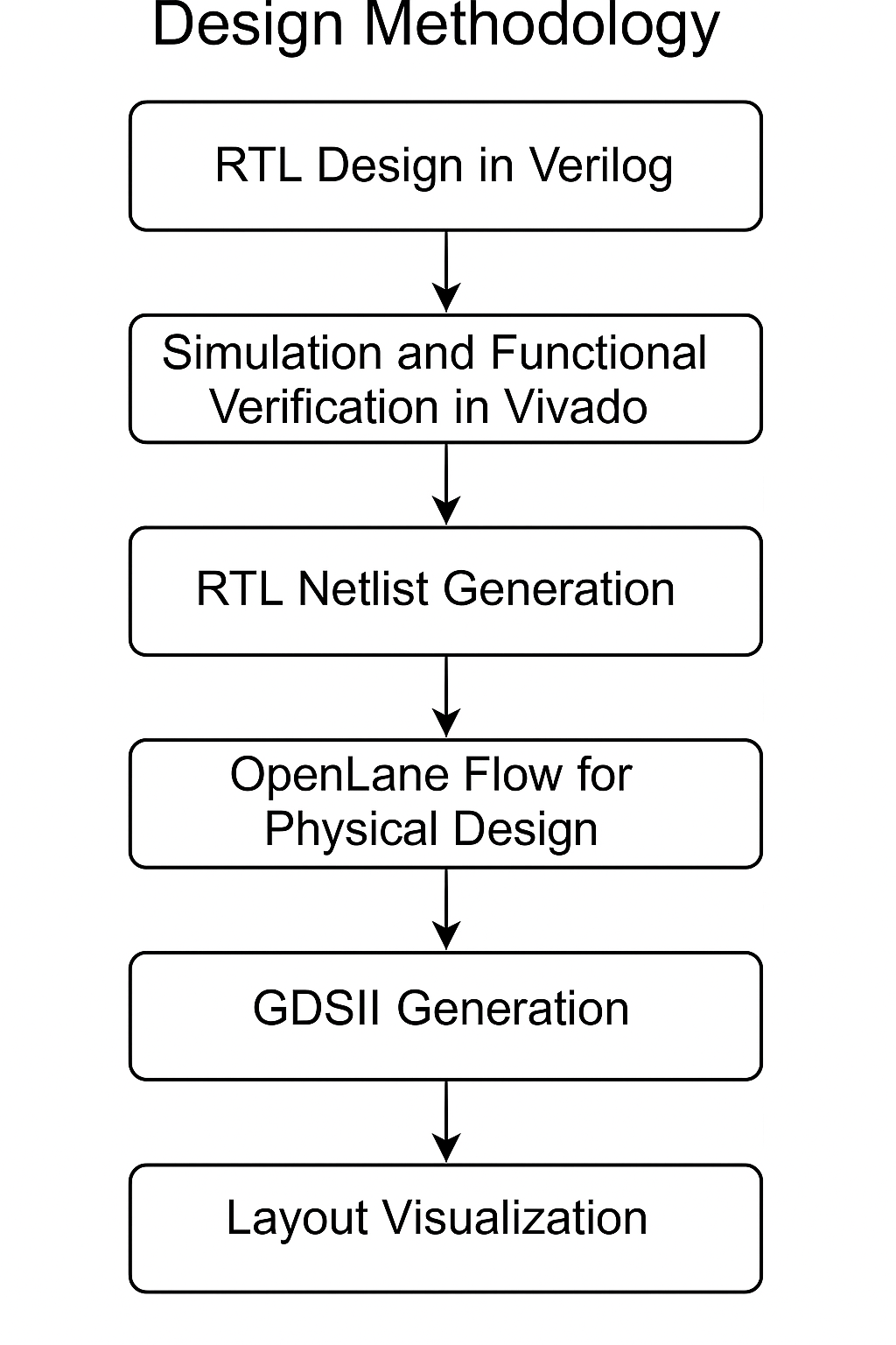
3.1 RTL Design in Verilog
The first step was writing the RTL (Register Transfer Level) code in Verilog for different parts of the FFT architecture. The following modules were created:
Butterfly Module – Performs the core FFT butterfly operation using complex arithmetic.
Floating Point Adder (Single-Cycle) – Used for accurate addition of real and imaginary parts.
Floating Point Multiplier – Used to multiply with twiddle factors (roots of unity).
FFT Control Path – Manages data flow and stage-by-stage operation of the FFT.
3.2 Simulation and Functional Verification in Vivado
After writing the code, the entire design was simulated using Xilinx Vivado:
A testbench was written to apply inputs and observe outputs.
The simulation confirmed correct working of the butterfly logic, control path, and floating-point arithmetic.
Any bugs or mismatches were resolved during this stage.
This ensured the design was functionally verified before moving to physical design.
3.3 RTL Netlist Generation
Once the design passed simulation, RTL netlist was generated in Vivado:
The synthesis tool inside Vivado converted the Verilog code into a gate-level representation.
This netlist was used as the input for back-end design using OpenLane.
3.4 OpenLane Flow for Physical Design
The .v Verilog netlist files were then placed inside the src/ directory of OpenLane. The following steps were performed using OpenLane:
Synthesis – Converts RTL to gate-level using the Sky130 standard cell library.
Floorplanning – Sets core area, pin positions, and placement rows.
Placement – Places logic gates (standard cells) in an optimized layout.
Clock Tree Synthesis (CTS) – Adds buffers and connects clock signals efficiently.
Routing – Connects all cells using metal layers.
GDSII Generation – Produces the final layout file (GDS format).
3.5 Layout Visualization
The final layout was viewed and verified using:
Magic VLSI Tool – To view layout, check for DRC (Design Rule Check) errors, and visualize routing.
KLayout – Used to load the .gds file and view the final chip layout clearly, layer by layer.
Both tools confirmed the successful generation of the physical layout of the 16-point FFT design.
4. Design and Simulation Results
This section provides an overview of the individual Verilog modules used in the design, followed by simulation results and RTL netlist verification.
4.1 Verilog Module Overview
The following Verilog files were used to build the complete 16-point FFT:
| File Name | Description |
| adder_single_cycle.v | Implements a single-cycle floating point adder for FFT operations. |
| butterflyy.v | Core butterfly computation unit using complex adders and multipliers. |
| fft_ctrl_sm.v | Control state machine managing the flow of data through FFT stages |
| fft_top.v | Top-level module that connects all FFT sub-modules |
| multiplier.v | Floating point multiplier used in butterfly and twiddle operations. |
| mem_32x16.v | Memory module for storing intermediate FFT results. |
4.2 Simulation Waveform
The entire FFT design was simulated in Xilinx Vivado using the fft_top.v module and relevant testbenches. The output waveform below shows the correct working of the butterfly module and data flow across FFT stages.
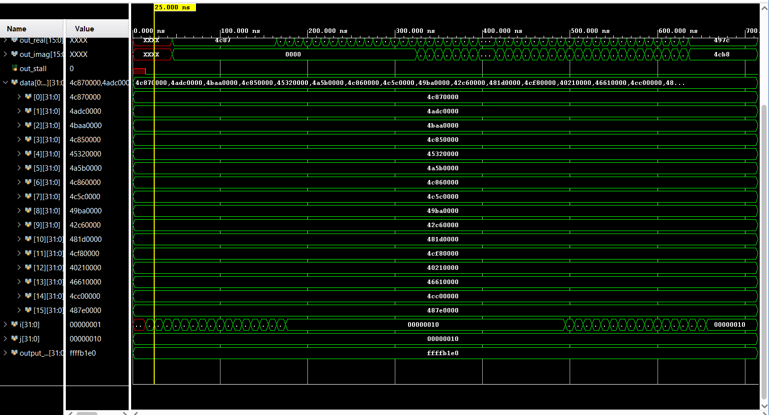
Figure 4.1: Simulation waveform of 16-point FFT showing correct output generation over clock cycles.
The waveform confirms that:
The input values are properly fetched from memory.
Twiddle factors are correctly applied using the w_lut.v module.
Outputs match expected values after each FFT stage.
4.3 RTL Netlist View
After simulation and synthesis, Vivado generated the RTL netlist.
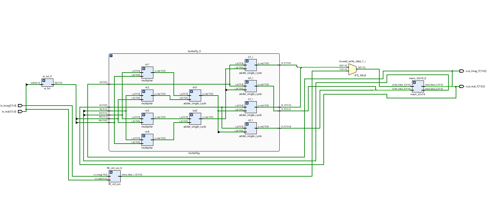
Figure 4.2: RTL-level synthesized netlist showing logic interconnections for FFT modules.
5. Physical Design and Layout Results
After verifying the RTL design through simulation and synthesis, the next step was to perform physical design using the OpenLane flow and view the final layout using Magic and KLayout.
5.1 Area Report (From Magic)
The final layout area was analyzed using Magic tool. The core dimensions and area are:
Width: 256.295 µm
Height: 267.015 µm
Total Area: ≈ 68434.61 µm²
In lambda units: 684,346,112 λ²
In internal units: 2,737,384,377 units²
Note: This area includes standard cells, interconnects, and I/O pins placed after routing.
5.2 Power Report
The power analysis was performed at the typical corner after routing. The results are:
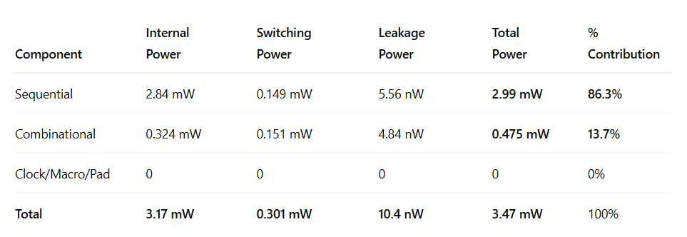
Most of the power is consumed by sequential elements (like flip-flops), which is typical in data path-heavy designs like FFT.
5.3 Timing Report
After completing the STA (Static Timing Analysis), the following timing metrics were obtained:
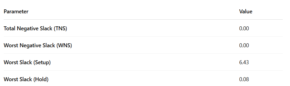
Conclusion: The design met all timing constraints with zero violations, indicating that both setup and hold requirements are comfortably met.
6. Layout Visualization
After generating the final GDSII file through OpenLane, the layout was verified and visualized using both KLayout and Magic tools. These tools provide a detailed graphical representation of the physical structure, which helps in inspecting standard cell placement, routing, and verifying DRC/LVS correctness.
6.1 KLayout View
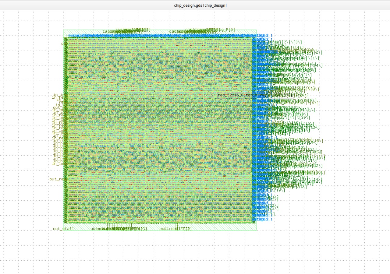
Figure 6.1: Layout view of the 16-point FFT design in KLayout
The above layout shows metal layers, vias, standard cell arrangement, and overall floorplan. This view is especially useful for cross-verification of GDS and for visual inspection of design quality.
6.2 Magic Layout View
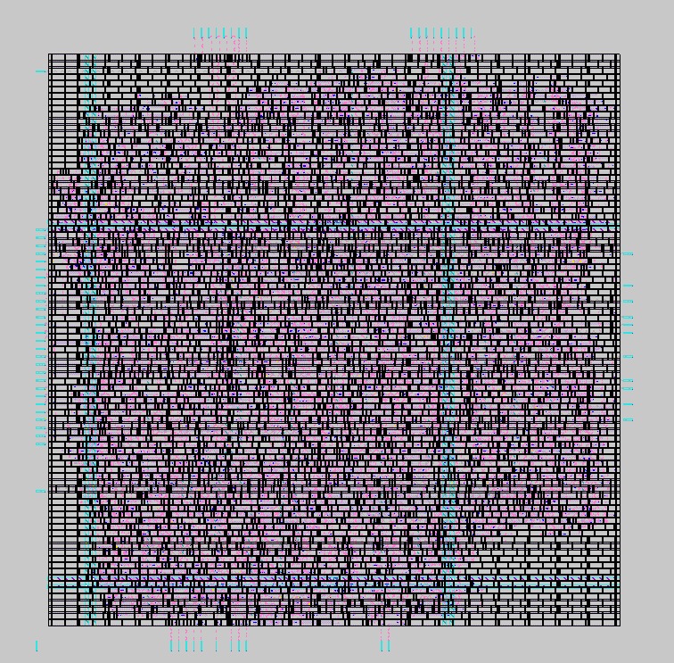
Figure 6.2: Layout view in Magic VLSI tool
The Magic layout provides insight into layer-wise representation and allows for DRC checks and layout editing. It was used to verify design rules and to ensure the correctness of placement and routing.
7. DRC and LVS Check Report
Post-layout verification is a crucial step in the ASIC design flow. This ensures the design is physically manufacturable and electrically correct. The following checks were performed using OpenLane, and the results confirm the successful completion of the flow with minimal issues.
.7.1 Design Rule Check (DRC)
The DRC was performed using Magic to ensure the layout adheres to the design rules specified for the 130nm Skywater PDK. The results are:
Total Magic DRC Violations: 0
The layout is DRC clean.
7.2 Layout Versus Schematic (LVS)
LVS was done to compare the netlist extracted from the layout against the original Verilog RTL netlist. This helps ensure functional equivalence between schematic and layout.
Number of Nets: 3403
LVS Status: The design is LVS clean.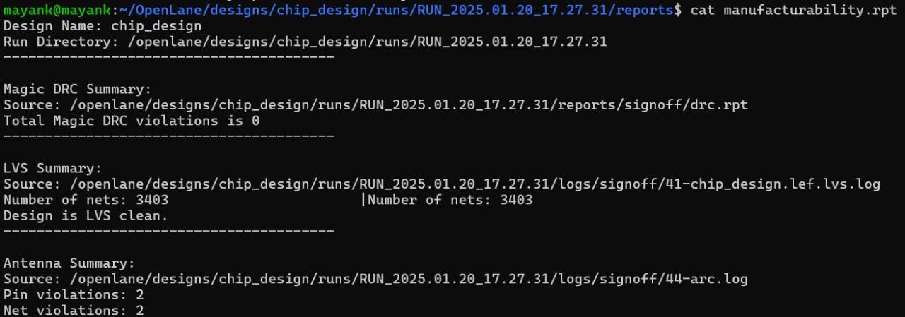
Figure 7.1: DRC and LVS report
8. Conclusion and Future Scope
8.1 Conclusion
This project successfully implemented a 16-point Fast Fourier Transform (FFT) using the ASIC design flow. Starting from writing the Verilog modules (including butterfly unit, adder, multiplier, control path, and memory units), the design was simulated in Vivado and then taken through the complete physical design process using OpenLane.
Key outcomes:
Functionality Verified: All modules passed functional simulation.
Physical Design Completed: RTL-to-GDSII flow achieved with no DRC or LVS errors.
Timing Closure: Zero TNS and WNS with positive slack.
Power Efficiency: Achieved low power consumption of ~3.47 mW, mostly dominated by sequential logic.
Area: Layout area of ~68434.609 μm² in 130nm technology node.
Manufacturability: The design passed all key checks, ensuring it is ready for tape-out with minimal fixes.
8.2 Future Scope
While this implementation is functional and clean, there are several directions in which the project can be extended:
🔁 Higher Point FFT: Extend the design to 32-point or 64-point FFT for applications requiring higher resolution frequency analysis.
🧮 Pipelined Architecture: Improve speed and throughput by using pipelined or parallel FFT structures.
⚡ Low Power Optimizations: Use clock gating, operand isolation, or voltage scaling to further reduce power consumption.
📦 Standard Cell Characterization: Customize standard cell libraries or use more advanced technology nodes (like 65nm) to improve area and performance.
📈 Post-Layout Simulation: Perform parasitic extraction and simulate using SPICE to evaluate the impact of wire delays.
🧠 Machine Learning Integration: Explore integrating FFT output into ML inference pipelines for real-time signal processing.
Report Information
Team Members
Team Members
Report Details
Created: April 7, 2025, 3:27 p.m.
Approved by: Omkar Patil [Diode]
Approval date: April 7, 2025, 10:37 p.m.
Report Details
Created: April 7, 2025, 3:27 p.m.
Approved by: Omkar Patil [Diode]
Approval date: April 7, 2025, 10:37 p.m.